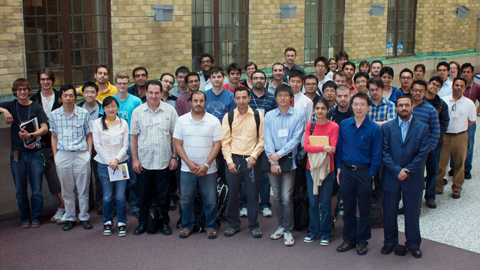
For nine days this month, 30 graduate students have been learning how to make nano-sized devices — devices with features that are thousands times smaller than the width of a human hair. Drawing participants primarily from U of T Engineering, the Connaught Summer Institute in Nanofabrication also attracted students from schools across Ontario, Quebec and British Columbia.
The summer institute was conceived by Professor Stewart Aitchison (ECE) who is also the Faculty’s Vice-Dean of Research, and hosted by U of T’s ECTI, which provides open research facilities for micro- and nanofabrication. Funding was received from the University’s Connaught Fund to foster connections and collaborations among students, postdoctoral fellows and other scholars.
In six, three-hour lab sessions, students learned how to operate equipment and perform the processes crucial to fabricating nano-scale devices. Dr. Aju Jugessur, a senior research associate with the ECTI, was part of the planning committee for the summer institute, and helped develop the training sessions.
“Many of us currently use computers, mobile phones, the Internet and other high-tech gadgets but probably have only vague ideas about the technologies involved in producing them. We are very comfortable with the concept of moving information around electronically, but the idea of literally moving or creating nano-sized features to build devices is still remote to many of us. This is what participants at the summer institute learned,” said Jugessur.
The unique nature of the training is what attracted Rahul Lodha, a doctoral student in materials engineering from the University of British Columbia.
“I’m currently working with both micro- and nano-size particles, and what I’ve been doing is to add the nano-particles to micro-structures. What I’ve learned here is how to combine the two,” said Lodha. “What’s of great interest to me is how the properties of a material change when you get to the nano scale. Nano-titanium dioxide can be used for water purification, because when regular light hits it, ultra-violet rays are emitted in the range required to purify water. But regular-sized titanium dioxide by itself doesn’t do this.”
In addition to the hands-on training, every morning from June 6-11 saw the students enjoy the insights of international experts — drawn from both academia and industry — in a wide variety of nanofabrication methods.
“We were pleased to involve three industrial partners in this summer institute. It helps students understand the connections and the collaborations that can stimulate new research and applications,” said Aitchison. “I’ve seen some estimates that North America will need two million nanotechnology workers over the next 10 years, so the skills we’re developing are economically very important.”


